Galaxy note3 n9005 smart phone repair reference schematic pcb board N900 schematics đồ tiết mạch sơ [view 39+] samsung note 4 schematic diagram
Schematic Samsung Galaxy Note 8 GT-N5100
Samsung note 8 sm-n950u pcb layout &teardown Schematic n920 skema cek solusion charger jalur Schematics samsung note 9 sm-n960n
[view 39+] samsung note 4 schematic diagram
Samsung galaxy note 3 sm-n900 schematicsSchematic samsung galaxy note 8 gt-n5100 Samsung galaxy note10+ schematicsNote the diagram below which shows a circuit created with a battery and.
Schematics note10 n975uSamsung note n900 galaxy sm dead support solution unofficial haldwani zone welcome site N900 galaxyFig. no 4.3 circuit diagram of the straightening and cutting machine.
Note samsung sm layout pcb n950u
Celulares esquemas eletricosUc3842 supply power charger battery switching 10a 15v Circuit current determine below figureShown circuit note figure consider currents calculate two emfs answers.
Schematic samsung galaxy note 5 sm-n920 charger data hardware solusionN770f schematics note10 Electronic components crazy fans: january 2013[view 39+] samsung note 4 schematic diagram.

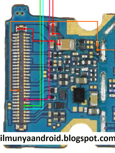
Schematic galaxy diagram note3 pcb n9005 maintenance reference repair manual smart phone board mouse zoom over
Diagrams crtSchematic schematics Schematics note10 n970fRedmi note diagram pro schematic.
Samsung galaxy note10 lite / sm-n770f schematicsSamsung galaxy note 3 sm-n900 dead solution ~ mobile support Solved consider the circuit shown in the figure. note thatSamsung galaxy note 3 sm-n900 lcd dispaly not working solution.
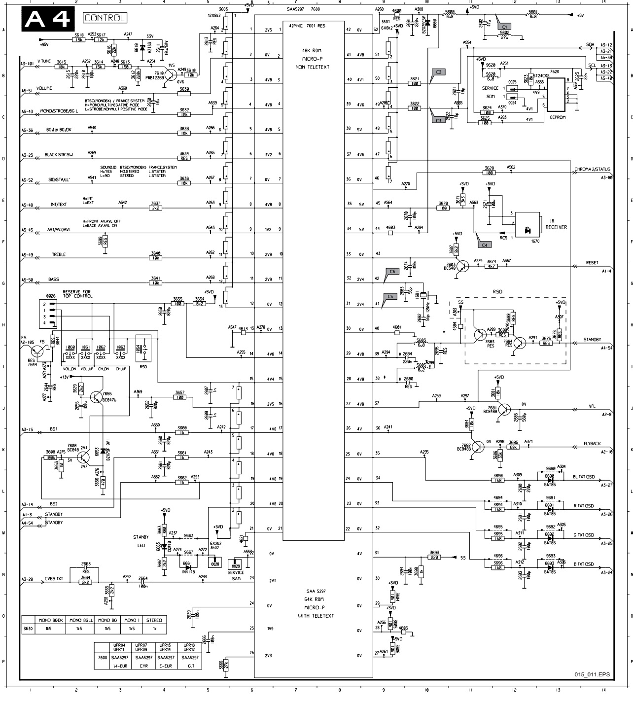
Schematic diagrams: philips 21pt1663 crttv circuit diagram (schematic)
Circuit diagram bulbs battery three note shows below which created solved chegg helpIn the circuit of the figure below determine the current Samsung galaxy note10 sm-n970f schematicsUc3842 switching power supply for battery charger 3-15v 10a.
Ams1117 circuit regulator supply power dual 3v voltage ams diagram board multi 0v note ldo electronic components fans crazy circuitsSchematics note10 Note samsung galaxy diagram ic circuit n9005 n900 disassembly youtu numberSamsung galaxy note 3 circuit diagram : r/mobilerepair.

Redmi note 3 pro schematic diagram & more
.
.
![[View 39+] Samsung Note 4 Schematic Diagram](https://1.bp.blogspot.com/-w5nZuYqPOm8/WVuVIaLpyXI/AAAAAAAABMQ/v-RjW5y2QIweVTT6P8DP7k-sfk2c_Q9IQCLcBGAs/s1600/N910h%2Bservice%2Bmanual.png)
Samsung Galaxy Note 3 Circuit Diagram : r/mobilerepair

Fig. No 4.3 CIRCUIT DIAGRAM OF THE STRAIGHTENING AND CUTTING MACHINE

Samsung Galaxy Note10 SM-N970F schematics

Note The Diagram Below Which Shows A Circuit Created With A Battery And
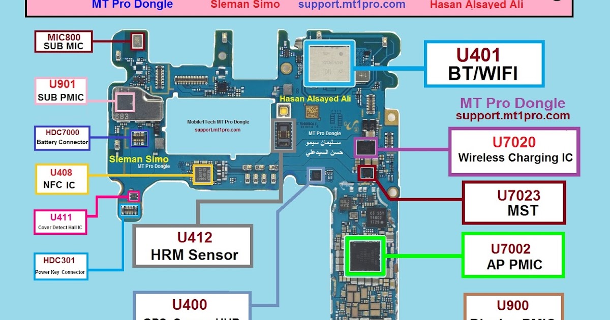
Samsung Note 8 SM-N950U Pcb Layout &Teardown
![[View 39+] Samsung Note 4 Schematic Diagram](https://i.pinimg.com/originals/d3/70/f1/d370f1b93da5ea97a13b682f2266a2ec.png)
[View 39+] Samsung Note 4 Schematic Diagram
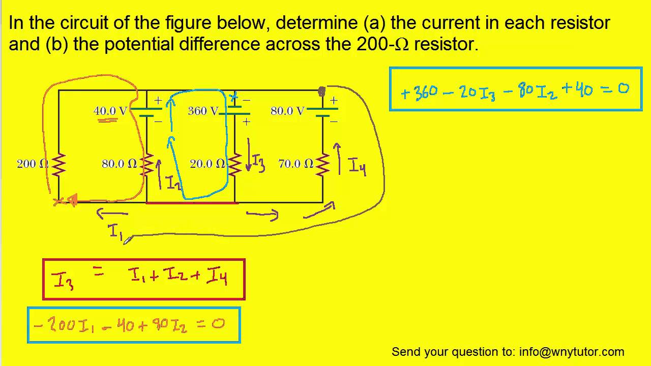
In the circuit of the figure below determine the current - YouTube
